PCB Laser Repair
In recent years, with the rapid development of electrical parts industry, the production scale of printed circuit board (PCB) has also shown a quantitative development trend, smaller electrical parts require higher density, higher precision PCB, which brings great challenges to the production quality control and poor detection, the high-precision smart phone board is one of the representatives. Since entering the 21st century, the global smart phone has developed rapidly, and the research and development of mobile communication has continued to develop in the direction of high density and ultra-thin. From the previous common High Density Interconnection (HDI) products with L/S (Line/Space ratio) of 100μm/100μm and above, to the current high precision, high density substrate L/S requirements of 50μm/50μm or lower, More and ore stringent requirements for L/S directly lead to a decline in PCB quality after the formation of graphics.
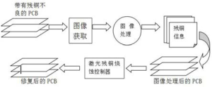
In the defects of formation of the pattern, the residual copper, exposure ghosting are the main defects. At present, the poor correction method is usually that the operator using the correction knife with the optical magnifying glass to correct. The steps are as follows: A) collect the images of the printed circuit board to be detected on site; B) The coordinates and area of residual copper are detected by the detection method of PCB residual copper defects; C) Manually determine whether it can be corrected by the correction knife; D) According to the position provided, the operator can accurately find the specific location of the inspected copper residue under the microscope. Then the operator should use appropriate correction tools and force to correct it, so as to avoid the damage caused by the correction process to other areas of the copper residue edge; E) Re-check PCB residual copper.
The main shortcomings of this manual use of correction knife to correct PCB residual copper are: The area of residual copper is required to be small, the thickness of residual copper is thin, and the thickness of the resin under the copper foil is thick enough to ensure that the operator will not lead to new bad after correction;While correcting the residual copper, it is also necessary to avoid the finished residual copper jumping to other areas and forming a new short circuit;The process is complex, it is not easy to train a mature operator, and the process required extremely professional operator;PCB board has entered the era of high precision and high density, manual operation has limitations in accuracy and repair, repair cost is high.
The thinner inter layer design puts higher requirements on the technical level of the operator, and with the development of PCB graphics to higher precision and higher density, the way of manual correction is becoming worse and worse in reliability and success rate.
Therefore, in order to solve the shortcomings of the above existing technologies, the laser correction PCB board defect method based on image detection has become the mainstream. On the basis of the original visual detection of PCB residual copper position, the method uses laser to correct the residual copper, instead of the traditional manual use of correction knife for residual copper correction, which solves the error caused by the operator, reduces the production cost, and improves the repair accuracy, repair efficiency and repair success rate of PCB residual copper.
Principle:
The laser PCB copper removal device obtains the PCB image through the image acquisition system, detects the coordinates and area of the PCB copper residue through the copper residue detection system, identifies and divides the area of the copper residue to be corrected. The laser illuminates this area, uses the thermal effect to ablate the residual copper defects, so as to realize the laser correction of the PCB defects.
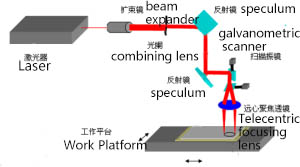
The MC series of sub nanosecond micro laser from RealLight is suitable for this application research. It has features of narrow pulse width, peak power, good beam quality, small size, stable performance and high performance. Compared with traditional nanosecond lasers and pico-second lasers, the residual copper can be removed quickly and accurately without damaging the PCB substrate. And because of its special energy and pulse width, it can be combined with laser transfer technology to repair the copper missing part quickly, that is, to solve the problem of PCB short circuit and open circuit at the same time.
Disclaimer: Part of the content of this article comes from the Internet, for the purpose of technical research and exchange, only for your reference and learning, welcome to let us know if the description is wrong or academic error. If copyright issues are involved, please contact us and we will verify and remove them as soon as possible.