The application of microchip lasers in the field of microscopic LIBS
The LIBS,Laser Induced Breakdown Spectroscopy instrument has been hidden in research laboratories.Due to the recent installation of LIBS payloads on Chinese Mars rovers, LIBS technology is gradually becoming known to the public.LIBS technology is the application of laser focusing on the surface of a substance to excite the substance to a plasma state through a peak power (>GW/cm2) laser, and analyze the composition and content of the substance through plasma emission spectroscopy. LIBS technology is currently widely used in alloys, ores, materials, agriculture, biology and other fields.
Laser induced breakdown spectroscopy (LIBS) technology can achieve in-situ, quantitative, and total elemental analysis of sample microregions, and is an important means of detecting the chemical composition of unknown substances. It is widely used in geological science, materials science, biomedical and other fields. The spatial resolution LIBS imaging technology has attracted increasing attention due to its ability to reveal the distribution of elements in the sample.

Reallight’s LIBS Instrument Machine
In the field of LIBS imaging research, chemical analysis of trace samples requires a spatial resolution of micrometer or even submicron level, and higher requirements are placed on the stability of the system. Higher requirements have also been put forward for the parameter performance of lasers.
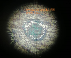
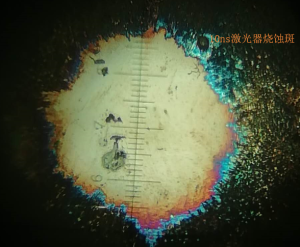
Recently, the team of Professor Xiu Junshan from Shandong University of Technology published a paper titled “Rapid micro-analysis of Al-In-Sn-O thin film using laser induced breakdown spectroscopy with picosecond laser pulses” in the Spectrochimica. The paper used micro LIBS technology to evaluate the performance of Al In Sn-O thin films by evaluating the element content under different preparation process parameters.In this paper, 350ps pulse width microplate laser of Reallight MCD series is used, and the resolution of transverse resolution is less than 50μm, and the resolution of film thickness is submicron level.
 Reallight-350ps pulse width thin film ablation spot

10ns pulse width laser ablation spot
The Reallight’s sub nanosecond microchip laser has a sub nanosecond pulse width and high beam quality (M2<1.2), making it easy to focus into μm-scale spot, achieving a power density of>10GW/cm2. The laser has high repetition rate, precise pulse synchronization control, and can achieve single pulse excitation control. The laser has a small size and high integration, making it very suitable for use in the field of microscopic LIBS.
Disclaimer: Some of the content in this article is from the internet and is intended for technical research and exchange. It is for reference and learning only. If there are any errors in the description or academic inaccuracies, please feel free to raise them in a timely manner. If there is any copyright issue, please contact us and we will verify and delete it as soon as possible.
References
Shiming Liu, Qing Gao, Junshan Xiu⁎, Zhao Li, Yunyan Liu,Spectrochimica Acta Part B[J],160(2019)105684
Huang Weihua, He Chunjing, Zhao Weiqian * *, Qiu Lirong *, Journal of Optics [J], Volume 40, Issue 24, December 2020.


